
Huawei has introduced its alternative to Moore's Law as it targets the development of 1.4nm chips.
Huawei's new strategy for chip development is advancing beyond 2nm
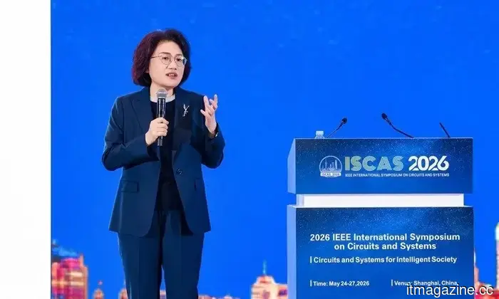
Huawei has unveiled what it considers a new direction for advanced semiconductor technology. During the 2026 IEEE International Symposium on Circuits and Systems in Shanghai, He Tingbo from Huawei introduced the company's Tau Scaling Law, a novel principle in semiconductor engineering that Huawei asserts can steer chip innovation as conventional Moore’s Law encounters physical and economic constraints.
The company claims that future high-end chips based on this methodology could achieve transistor densities of 14 angstroms, or 1.4nm, by 2031.
Huawei's impact on the chip industry
He Tingbo presented during Huawei's keynote at the IEEE event.
While 1.4nm sounds impressive, it's crucial to note that "equivalent" is the key term. Huawei is not claiming to have obtained access to the world’s most sophisticated chip manufacturing tools, and it has not yet released any independent performance metrics. Currently, China's leading chip manufacturing capability is generally perceived to be around 7nm, which is exemplified by the chip in Huawei’s tri-fold smartphone. The company's strategy aims to enhance performance through system-level efficiency instead of solely depending on smaller transistors.
The Tau Scaling approach emphasizes reducing the time required for signals and data to traverse through chips and computing systems, utilizing Huawei's new LogicFolding architecture. This technology effectively shortens critical path wiring, lowers signal propagation load, and enhances both transistor density and circuit efficiency.
Which chips will be the first to implement this technology?
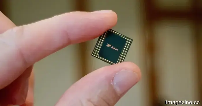
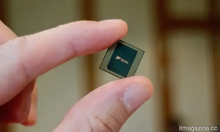
Huawei's chip arm, HiSilicon, plans to integrate this technology into its latest generation of Kirin chips, expected to launch in the fall of 2026 featuring the new LogicFolding technology. The company also states that it has designed and mass-produced 381 chips over the last six years based on Tau Scaling, covering various applications such as smartphones and AI computing.
Additionally, Huawei intends to apply LogicFolding to Ascend AI chips by 2030, alongside large AI clusters in data centers. While the 1.4nm target is attention-grabbing, the Ascend chips hold more significance. Given that Chinese firms are seeking alternatives to Nvidia's hardware, which faces restrictions in the region, Huawei's AI chips are becoming increasingly crucial. As reported by Reuters, Nvidia CEO Jensen Huang recently mentioned that the company has "largely conceded" the AI chip market in China to Huawei.
Due to US export controls limiting Chinese access to advanced lithography systems and other essential semiconductor technologies, progressing toward frontier nodes through traditional means is becoming much more challenging. TSMC currently utilizes 2nm technology and aims for 1.4nm mass production by 2028, while Huawei is attempting to achieve similar densities through a different design approach. Therefore, the company is clearly not depending on Moore’s Law or the easing of US restrictions to dictate how far its chip advancements can go.





Other articles
 Copilot is receiving a sidebar design for Windows 11, similar to Gemini in Chrome.
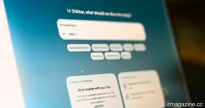
Copilot is set to receive a dockable sidebar in Windows 11, functioning similarly to Gemini in Chrome, an approach that Microsoft previously attempted and abandoned.
Copilot is receiving a sidebar design for Windows 11, similar to Gemini in Chrome.
Copilot is set to receive a dockable sidebar in Windows 11, functioning similarly to Gemini in Chrome, an approach that Microsoft previously attempted and abandoned.
 Microsoft will allow users to remove the Copilot app as part of its ongoing cleanup for Windows 11.
The most recent update to Windows 11 from Microsoft brings new options for permanently eliminating Copilot via Group Policy, alterations to the Registry, and conventional uninstallation methods.
Microsoft will allow users to remove the Copilot app as part of its ongoing cleanup for Windows 11.
The most recent update to Windows 11 from Microsoft brings new options for permanently eliminating Copilot via Group Policy, alterations to the Registry, and conventional uninstallation methods.
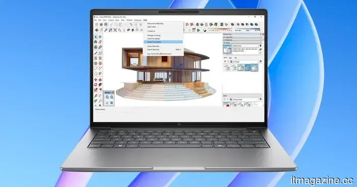 HP's latest ZBook workstations feature AI chips, Blackwell GPUs, and eye-popping price tags.
HP has introduced new ZBook workstation laptops that are equipped with Ryzen AI processors, high-quality displays, and top-tier configurations designed for creators and professional users.
HP's latest ZBook workstations feature AI chips, Blackwell GPUs, and eye-popping price tags.
HP has introduced new ZBook workstation laptops that are equipped with Ryzen AI processors, high-quality displays, and top-tier configurations designed for creators and professional users.
 Microsoft will finally allow you to remove Copilot.
The April 2026 update for Windows 11 introduces an official option to uninstall Copilot, following the fact that only 3.3% of eligible users decided to pay for it and after requests from administrators for removal controls.
Microsoft will finally allow you to remove Copilot.
The April 2026 update for Windows 11 introduces an official option to uninstall Copilot, following the fact that only 3.3% of eligible users decided to pay for it and after requests from administrators for removal controls.
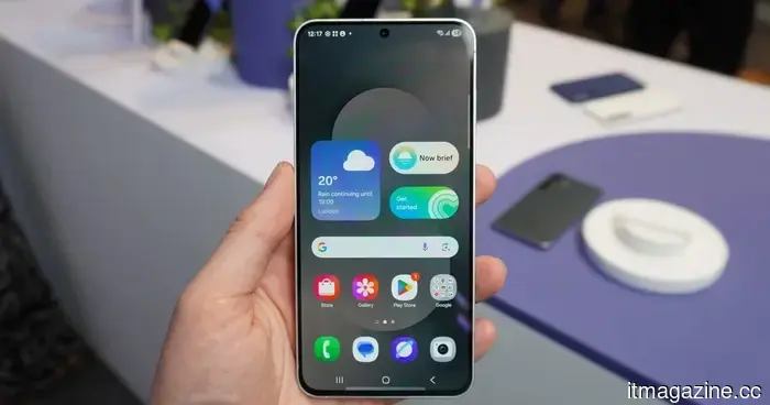 The upcoming budget flagship from Samsung has just been revealed, and here's a glimpse of its design.
Case renders for the Galaxy S26 FE have emerged online, showcasing its design and potential color choices several months before its anticipated release in October.
The upcoming budget flagship from Samsung has just been revealed, and here's a glimpse of its design.
Case renders for the Galaxy S26 FE have emerged online, showcasing its design and potential color choices several months before its anticipated release in October.
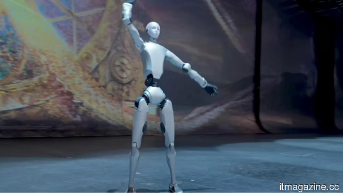 China has issued ID codes to over 28,000 humanoid robots.
China implemented a national robot identification system that assigns a 29-character code to each humanoid robot, allowing for tracking from the factory to the scrapyard. So far, 28,000 robots have been registered.
China has issued ID codes to over 28,000 humanoid robots.
China implemented a national robot identification system that assigns a 29-character code to each humanoid robot, allowing for tracking from the factory to the scrapyard. So far, 28,000 robots have been registered.
Huawei has introduced its alternative to Moore's Law as it targets the development of 1.4nm chips.
Huawei's Tau Scaling Law redirects the focus of the chip competition from merely reducing transistor size to enhancing signal speed, with the company confidently targeting a density equivalent to 1.4nm by 2031.