IBM claims to have developed the first chip technology with a size under 1nm.
IBM has revealed that it has created the world's first sub-1nm chip technology, featuring a transistor architecture at what it refers to as the 0.7nm, or 7-angstrom, node. This achievement is a significant milestone that the semiconductor industry has been striving to reach for years, and such a claim requires careful consideration, as a node designation is no longer a measurement of anything tangible.
The technology is based on a design called “nanostack,” which IBM describes as the industry's first three-dimensional, nanosheet-based transistor architecture. Instead of arranging transistors on a flat surface and reducing the space between them, nanostack vertically stacks and staggers them, utilizing 3D sequential integration to accommodate more transistors in the same area.
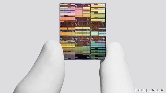
This approach also allows engineers to utilize various material combinations in each layered stack, enabling independent tuning of each transistor's performance and power. The key figure here is transistor density. IBM claims that the chip contains nearly 100 billion transistors on a piece of silicon the size of a fingernail, nearly double the density of the 2nm chip introduced in 2021.
According to the company's published findings, this new node provides up to 50% greater performance and up to 70% improved energy efficiency compared to the 2nm generation. However, these figures are projections based on research results, rather than actual numbers from a commercial product, and they describe different operational scenarios instead of a single chip achieving both metrics simultaneously.
Supporting research backs up this announcement. In studies presented at VLSI 2026, IBM stated that nanostack offers 40% scaling in SRAM, a critical on-chip memory type that has historically resisted miniaturization, which is crucial for the high-bandwidth demands of AI applications. IBM also claims to have validated the architecture using dielectric bonding within CMOS integration and demonstrated a functioning CMOS inverter, indicating that the structure can indeed be physically constructed and is capable of switching, not just simulated.
“With our new nanostack architecture, we’re not merely creating smaller transistors; we’re transforming the way chips are constructed,” stated Jay Gambetta, director of IBM Research.
This context is important, as the industry has moved beyond literal dimensional scaling for some time now. A “0.7nm” node does not imply that any feature measures 0.7 nanometers; it serves as a generational identifier. What IBM is asserting is that nanostack allows logic to enter the territory below the 1nm node, which they describe as angstrom-scale, where dimensions approach the size of individual atoms.
The research was conducted at the Albany research facility in upstate New York, which is set to house a High-NA EUV lithography tool from ASML, considered essential for printing circuits at these small dimensions. IBM has acknowledged contributors such as Lam Research, Tokyo Electron, and SCREEN Semiconductor Solutions, and mentioned its recent establishment of Anderon, a dedicated quantum foundry, as part of its efforts to maintain advanced chip manufacturing domestically.
ASML’s High-NA equipment has sparked debate in the industry regarding costs, with TSMC initially expressing skepticism about the pricing.
An important caveat accompanies every IBM chip announcement: the company divested its manufacturing operations to GlobalFoundries in 2014, and now focuses on developing technology to be licensed and fabricated by others. Thus, this represents a research milestone rather than a market-ready product. IBM anticipates that a path to production could take as long as five years, a considerable timeline during which much could change. Currently, IBM has a functioning structure in the lab, a roadmap that it claims provides the industry with another decade of scaling, and a node name that serves primarily as an expression of intent.
Other articles
 The iPhone 18 Pro may not be excessively priced, but I would still advise caution.
Increasing costs for RAM and storage continue to pose a challenge for Apple; however, J.P. Morgan thinks that the price hike for the iPhone 18 Pro might be less significant.
The iPhone 18 Pro may not be excessively priced, but I would still advise caution.
Increasing costs for RAM and storage continue to pose a challenge for Apple; however, J.P. Morgan thinks that the price hike for the iPhone 18 Pro might be less significant.
 According to reports, Apple has addressed the problems with the hinge of the foldable iPhone, so you can feel a bit more at ease now.
Apple has allegedly addressed the majority of the hinge problems that raised concerns about delays for its first foldable iPhone, with mass production expected to start next month.
According to reports, Apple has addressed the problems with the hinge of the foldable iPhone, so you can feel a bit more at ease now.
Apple has allegedly addressed the majority of the hinge problems that raised concerns about delays for its first foldable iPhone, with mass production expected to start next month.
 Two additional researchers from Gemini are departing Google to join Anthropic.
Jonas Adler and Alexander Pritzel, both significant contributors to Gemini, are departing from Google to join Anthropic, marking the latest in a series of prominent AI departures.
Two additional researchers from Gemini are departing Google to join Anthropic.
Jonas Adler and Alexander Pritzel, both significant contributors to Gemini, are departing from Google to join Anthropic, marking the latest in a series of prominent AI departures.
 South Korean semiconductor stocks rise following Micron's positive earnings report.
On June 25, Samsung and SK Hynix drove a 4% increase in the KOSPI following Micron's impressive quarter and forecast, which boosted optimism regarding AI memory demand.
South Korean semiconductor stocks rise following Micron's positive earnings report.
On June 25, Samsung and SK Hynix drove a 4% increase in the KOSPI following Micron's impressive quarter and forecast, which boosted optimism regarding AI memory demand.
 Amazon plans to invest an additional $13 billion in cloud and AI in India by 2030.
Amazon plans to invest an additional $13 billion in cloud and AI infrastructure in India, raising its commitment for the 2026-2030 period to $48 billion, as announced during Jassy's meeting with Modi.
Amazon plans to invest an additional $13 billion in cloud and AI in India by 2030.
Amazon plans to invest an additional $13 billion in cloud and AI infrastructure in India, raising its commitment for the 2026-2030 period to $48 billion, as announced during Jassy's meeting with Modi.
 Nothing provides a sneak peek of the Phone 4b before its launch on July 7.
The design of the upcoming Phone 4b has not been disclosed, but it is said to combine the unibody structure of the 4a Pro with the Glyph Bar from the regular 4a.
Nothing provides a sneak peek of the Phone 4b before its launch on July 7.
The design of the upcoming Phone 4b has not been disclosed, but it is said to combine the unibody structure of the 4a Pro with the Glyph Bar from the regular 4a.
IBM claims to have developed the first chip technology with a size under 1nm.
IBM introduced a 0.7nm chip utilizing a new 3D 'nanostack' design, containing almost 100 billion transistors on a chip the size of a fingernail.