Huawei's 'chip queen' reveals the Tau Scaling Law.
Huawei’s semiconductor leader, He Tingbo, made her public reappearance after a seven-year hiatus to present the Tau Scaling Law and LogicFolding architecture. The company asserts it can achieve chip densities equivalent to 1.4 nm by 2031 without relying on EUV lithography, but it faces significant challenges related to heat management, EDA tools, and yield rates.
For seven years, He Tingbo remained out of sight. The head of Huawei’s semiconductor division, often referred to as the company’s “chip queen,” withdrew from the public eye in 2019 following the U.S. decision to cut Huawei off from advanced technologies. Her absence became emblematic of Huawei's struggle for survival. This changed on May 25 at the IEEE International Symposium on Circuits and Systems in Shanghai, where she delivered a keynote speech titled “New Semiconductor Path in Practice.”
A new principle for a new era
He introduced the “Tau (τ) Scaling Law,” which shifts the focus from shrinking transistors geometrically to measuring progress by signal-propagation time. Named after the Greek symbol for propagation delay, this law concentrates on minimizing signal travel time within devices and circuits instead of reducing transistor size.
Huawei claims that by 2031, it will develop high-end chips that achieve transistor densities comparable to a 1.4-nanometer process without the EUV lithography equipment that is currently restricted by U.S. sanctions. The company says it has already designed and produced 381 chips based on this principle over the last six years.
Analysts suggest that the fundamental physics behind this approach is not entirely original. Brady Wang, an associate director at Counterpoint Research, indicated that Design-Technology Co-Optimisation techniques have been globally used for years and that Huawei is “leveraging design and packaging innovations to achieve benefits typically linked to more advanced process nodes.” Nonetheless, consolidating these efforts into a cohesive law is significant. CGTN reported that semiconductor researchers likened it to Gordon Moore’s groundbreaking observation from 1965.
LogicFolding: more than just 3D stacking
The practical realization of the Tau law is LogicFolding, a proprietary architecture that transforms standard flat circuit designs into vertical, stacked configurations. Although some critics have dismissed it as simply a variation of advanced 3D packaging, He Tingbo emphasized the distinction: traditional 3D stacking connects prefabricated chips, while LogicFolding reimagines a single chip’s internal design from scratch.
According to Tom’s Hardware, this design increases transistor density by 53.5%, adding 238 million transistors per square millimeter of chip area. Nvidia CEO Jensen Huang called the architecture “a breakthrough for Huawei,” but noted it does not currently threaten TSMC’s manufacturing supremacy, highlighting that “TSMC and Taiwan have had this technology for 10 years.”
Born from restrictions
Huawei’s semiconductor pursuit under sanctions is a narrative of turning limitations into motivation. In 2019, He Tingbo revealed an internal plan outlining a “spare tyre” strategy to mitigate risks, which Huawei had secretly prepared in anticipation of this situation.
At the IEEE forum, she expressed her profound frustration, stating that she felt “as if there was really no way out.” Her moment of realization was inspired by Dujiangyan, a 2,000-year-old irrigation system in Sichuan that was constructed without modern tools. She began perceiving sanctions as engineering challenges to be overcome rather than obstacles to accept.
This resilience bore fruit. In September 2023, Huawei released the Mate 60 Pro smartphone, powered by the 5G-compatible Kirin 9000s. A teardown by TechInsights confirmed that the chip was fabricated by SMIC using a 7nm process, pushing DUV lithography technologies to their limits without any EUV equipment.
Huawei subsequently unveiled a three-year roadmap for its Ascend AI processors to serve as domestic alternatives to Nvidia, with the Ascend 950 set for 2026, the 960 for 2027, and the 970 for 2028. Founder Ren Zhengfei told People’s Daily: “There is actually no need to worry about the chip issue.” He added, “By using methods like stacking and clustering, computing performance is comparable to the state-of-the-art level.”
Nvidia CEO Jensen Huang confirmed that Nvidia’s share of China’s high-end AI chip market has plummeted from 95% to nearly zero, a comment he made at the Citadel Securities Future of Global Markets event in October 2025. Huawei’s rotating chairman Xu Zhijun remarked on the irony: “If the United States hadn’t forced our country, companies, and industry, we wouldn’t have done something like this. We are also grateful to the U.S. for enabling our country’s semiconductor industry chain to truly grow.”
The evolving geopolitical landscape
Washington continues to focus on preventing China from accessing advanced lithography technologies. In response, Beijing is investing billions into developing domestic
Other articles
 Airalo and the Emergence of eSIM Travel: A More Intelligent Method to Remain Connected While Traveling Abroad
International travel relies on connectivity more than it ever has. Whether it's finding your way in new cities, handling bookings, or keeping in contact with family back home, dependable mobile data is crucial. Here's how Airalo is assisting travelers in staying connected in over 200 countries and regions using the convenience of eSIM technology.
Airalo and the Emergence of eSIM Travel: A More Intelligent Method to Remain Connected While Traveling Abroad
International travel relies on connectivity more than it ever has. Whether it's finding your way in new cities, handling bookings, or keeping in contact with family back home, dependable mobile data is crucial. Here's how Airalo is assisting travelers in staying connected in over 200 countries and regions using the convenience of eSIM technology.
 YouTube's AI content cleanup is penalizing human creators who have never revealed their identities.
YouTube has terminated 16 channels that collectively had 4.7 billion views and is experimenting with viewer surveys to identify low-quality AI content. However, faceless creators argue that this enforcement also punishes them.
YouTube's AI content cleanup is penalizing human creators who have never revealed their identities.
YouTube has terminated 16 channels that collectively had 4.7 billion views and is experimenting with viewer surveys to identify low-quality AI content. However, faceless creators argue that this enforcement also punishes them.
 Facebook has introduced an AI search engine that retrieves answers from posts in your Groups and Reels.
Meta has introduced AI Mode on Facebook, which is an AI search tool that gathers answers from public posts in Groups, Reels, and Marketplace listings.
Facebook has introduced an AI search engine that retrieves answers from posts in your Groups and Reels.
Meta has introduced AI Mode on Facebook, which is an AI search tool that gathers answers from public posts in Groups, Reels, and Marketplace listings.
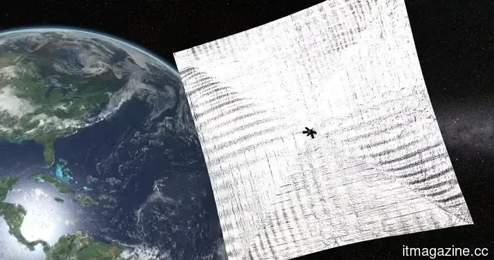 Lightsails have encountered another obstacle on their journey toward interstellar travel.
A recent study indicates that laser-powered interstellar lightsails could encounter an unnoticed efficiency issue as the light used to propel them begins to act in a less favorable manner.
Lightsails have encountered another obstacle on their journey toward interstellar travel.
A recent study indicates that laser-powered interstellar lightsails could encounter an unnoticed efficiency issue as the light used to propel them begins to act in a less favorable manner.
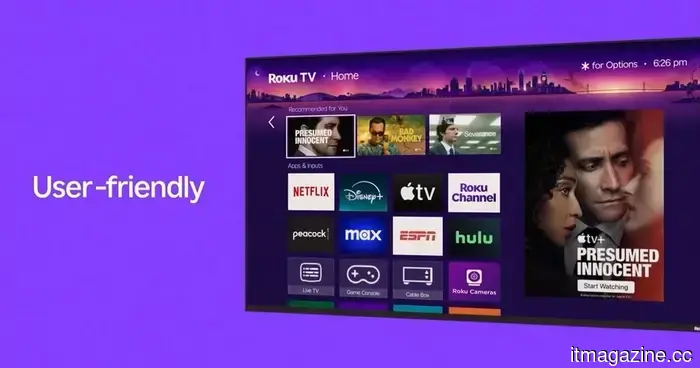 After twenty years of independence, Roku is being acquired for $22 billion by this company.
Fox is acquiring Roku in a monumental $22 billion agreement that has the potential to transform the streaming industry, aligning one of the largest content libraries in television with a platform that reaches over 100 million homes globally.
After twenty years of independence, Roku is being acquired for $22 billion by this company.
Fox is acquiring Roku in a monumental $22 billion agreement that has the potential to transform the streaming industry, aligning one of the largest content libraries in television with a platform that reaches over 100 million homes globally.
 YouTube's AI content cleanup is penalizing the human creators who chose not to show their faces.
YouTube has shut down 16 channels that accumulated 4.7 billion views and is experimenting with viewer surveys to identify low-quality AI content. However, creators without a visible presence argue that this action unfairly affects them as well.
YouTube's AI content cleanup is penalizing the human creators who chose not to show their faces.
YouTube has shut down 16 channels that accumulated 4.7 billion views and is experimenting with viewer surveys to identify low-quality AI content. However, creators without a visible presence argue that this action unfairly affects them as well.
Huawei's 'chip queen' reveals the Tau Scaling Law.
He Tingbo has returned to introduce a new scaling law and the LogicFolding architecture, which Huawei asserts can achieve 1.4nm chip density by 2031, all without the use of EUV lithography.