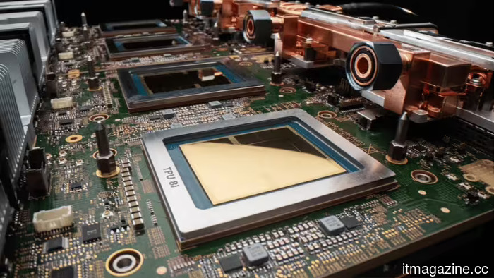
Google unveils the Ironwood TPU and offers a preview of its eighth generation, which is divided into training and inference chips at TSMC's 2nm technology.
Summary: At Cloud Next 2026, Google announced the general availability of Ironwood, its seventh-generation TPU, and provided a preview of its eighth-generation architecture: TPU 8t (Sunfish), a training chip designed by Broadcom, and TPU 8i (Zebrafish), an inference chip developed by MediaTek, both intended for TSMC's 2nm node and scheduled for late 2027. Ironwood offers 4.6 petaFLOPS per chip and 42.5 exaFLOPS in a superpod of 9,216 chips. This marks the first time Google has created separate chips specifically for training and inference, with Anthropic becoming the primary customer with a deal for 3.5 gigawatts of compute by 2027.
On Tuesday at Google Cloud Next in Las Vegas, Google made Ironwood, its seventh-generation Tensor Processing Unit, available to cloud clients, branding it “the first Google TPU for the age of inference.” This represents what could be the most significant infrastructure investment in the company's history. Ironwood boasts 4.6 petaFLOPS of peak FP8 computing power per chip, which is approximately four times the performance of its predecessor, Trillium, featuring 192 gigabytes of HBM3e memory and a memory bandwidth of 7.37 terabytes per second. A single Ironwood superpod connects 9,216 chips into an integrated system that delivers 42.5 exaFLOPS of computing power, significantly surpassing El Capitan, the world's most powerful supercomputer, by more than 24 times.
Ironwood’s specifications position it as a true competitor to Nvidia’s Blackwell B200, with both providing around 4.5 to 4.6 petaFLOPS of FP8 compute and 192 gigabytes of HBM. Nvidia has an advantage in single-device interconnect bandwidth at 14.4 terabits per second via NVLink, compared to Ironwood’s 9.6 terabits over ICI, and supports FP4 precision, which increases inference throughput for quantised models—a feature that Ironwood does not support. Google, however, has the upper hand at the cluster level with its superpod architecture and energy efficiency, which gives it roughly double the performance per watt of Trillium and 2.8 times that of Nvidia’s H100, along with the cost advantages of running inference tasks on custom silicon rather than general-purpose GPUs.
The focus on inference instead of training illustrates a strategic pivot. Training a state-of-the-art model is a capital expense that occurs once, spanning weeks or months, while inference—the operation of that model in response to user queries—is an ongoing operational expense that grows with demand and is continuous. Google aims to double its AI serving capacity every six months to satisfy demand across its services like Gemini, Search, YouTube, and Gmail. At this growth rate, inference costs become the largest variable in AI economics, and the organization that creates the most efficient and cost-effective inference hardware stands to gain the margins typically held by Nvidia.
Ironwood is designed for predominant production AI workloads, including large language model inference, mixture-of-experts architectures, diffusion models, and reinforcement learning. Each chip's 192 gigabytes of HBM3e allows for larger model shards in memory, minimizing the need to split a model across various chips. The 256-by-256 matrix multiply unit array, featuring 65,536 multiply-accumulate operations per cycle, is optimized for the dense linear algebra prevalent in transformer inference. Additionally, Google will make its internal Pathways distributed runtime available to cloud clients for the first time, facilitating multi-host inference with dynamic scaling across Ironwood pods.
As it launched Ironwood, Google also unveiled its eighth-generation TPU architecture, marking the first split into two distinct types. TPU 8t, codenamed Sunfish, is a training accelerator engineered with Broadcom. It comprises two compute dies, one I/O chiplet, and eight stacks of 12-high HBM3e, offering approximately a 30% increase in memory bandwidth over Ironwood's eight-high stacks. TPU 8i, codenamed Zebrafish, serves as an inference accelerator developed with MediaTek, featuring a single compute die, one I/O die, and six stacks of HBM3e for a configuration aimed at providing inference at a cost that is 20 to 30% lower than what the training variant offers. Both chips will be manufactured on TSMC’s 2-nanometre process node and are slated for late 2027.
This division is a pivotal architectural choice in Google’s TPU evolution. Previously, each generation merged training and inference capabilities in a single chip. The decision to separate acknowledges a truth the industry has realized over years: training and inference workloads are fundamentally distinct. Training requires maximum computational density and memory bandwidth for processing trillions
Other articles
 YouTube is addressing celebrity deepfakes with new technology for detecting AI-generated likenesses.
YouTube is broadening its AI technology for likeness detection to include talent agencies, managers, and celebrities, aiming to assist in the identification and removal of deepfakes.
YouTube is addressing celebrity deepfakes with new technology for detecting AI-generated likenesses.
YouTube is broadening its AI technology for likeness detection to include talent agencies, managers, and celebrities, aiming to assist in the identification and removal of deepfakes.
 Wide foldables seem like a solution to numerous issues, and I'm eager to see Apple take a shot at it.
The more I examine wide foldables like those from Huawei, the more I believe that Apple's initial foldable could address some of the most frustrating compromises of this format.
Wide foldables seem like a solution to numerous issues, and I'm eager to see Apple take a shot at it.
The more I examine wide foldables like those from Huawei, the more I believe that Apple's initial foldable could address some of the most frustrating compromises of this format.
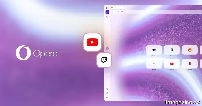 Opera One enhances video watching by offering a 500% volume boost, upgraded Picture-in-Picture (PiP) functionality, and support for streaming through the sidebar.
Opera One now enables users to pin YouTube and Twitch in the sidebar, increase tab volume to 500%, and utilize an updated picture-in-picture mode for video calls.
Opera One enhances video watching by offering a 500% volume boost, upgraded Picture-in-Picture (PiP) functionality, and support for streaming through the sidebar.
Opera One now enables users to pin YouTube and Twitch in the sidebar, increase tab volume to 500%, and utilize an updated picture-in-picture mode for video calls.
 Xbox Game Pass has just become more affordable, and I have no objections to the change that comes with it.
Xbox Game Pass lowers its price but loses day-one access to Call of Duty. Is this a strategic reset or a decline in value? Here’s what’s different, the significance of these changes, and how gamers are responding.
Xbox Game Pass has just become more affordable, and I have no objections to the change that comes with it.
Xbox Game Pass lowers its price but loses day-one access to Call of Duty. Is this a strategic reset or a decline in value? Here’s what’s different, the significance of these changes, and how gamers are responding.
 The Devil May Cry Season 2 trailer featuring the clash between Dante and Vergil has captured our full attention.
Netflix has released a trailer for Season 2 of Devil May Cry, hinting at an intense confrontation between Dante and Vergil while also introducing two significant villains.
The Devil May Cry Season 2 trailer featuring the clash between Dante and Vergil has captured our full attention.
Netflix has released a trailer for Season 2 of Devil May Cry, hinting at an intense confrontation between Dante and Vergil while also introducing two significant villains.
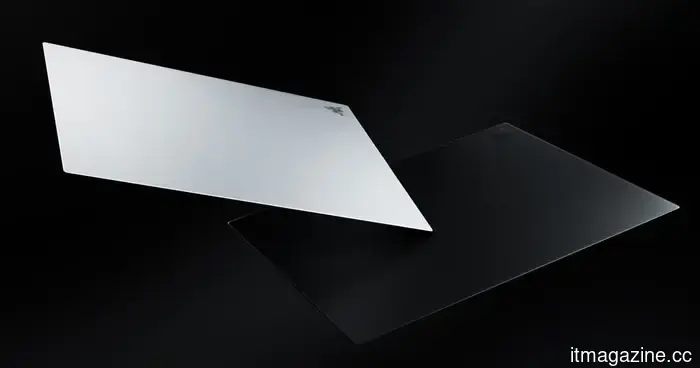 Razer has created the thinnest glass mouse pad in the world, and your wrists will appreciate it.
Razer's Atlas Pro is the thinnest glass gaming mouse mat globally, measuring only 1.9mm, and it aims to enhance the comfort of your gaming setup.
Razer has created the thinnest glass mouse pad in the world, and your wrists will appreciate it.
Razer's Atlas Pro is the thinnest glass gaming mouse mat globally, measuring only 1.9mm, and it aims to enhance the comfort of your gaming setup.
Google unveils the Ironwood TPU and offers a preview of its eighth generation, which is divided into training and inference chips at TSMC's 2nm technology.
Google's Ironwood TPU is operational, delivering 4.6 petaFLOPS per chip. The eighth generation is divided into two parts: Broadcom for training and MediaTek for inference, both manufactured at 2nm, set to launch in late 2027.