

SK Hynix has started construction on a $4 billion memory packaging facility in Indiana.
SK Hynix has commenced construction on a plant in West Lafayette, Indiana, with an investment exceeding $4 billion. This will be the company's first facility in the United States dedicated to packaging high-bandwidth memory, with production expected to begin in the latter half of 2029. In contrast, Intel's similar assembly and testing operation near Wroclaw was canceled last year despite previously approved state assistance.
The new SK Hynix plant will cover 133.5 acres and is projected to create around 1,000 jobs. Although production dates are far off, CEO Kwak Noh-Jung mentioned that the cleanroom is slated to open by October 2028, with mass production of the next-generation HBM commencing in late 2029.
The significance of this plant lies more in its function than its cost. Advanced packaging technology integrates completed chips into a single unit, which is essential for the effectiveness of Nvidia's highest-performing accelerators.
The U.S. government is contributing to the effort, as the CHIPS and Science Act allocates up to $458 million in direct support and up to $500 million in loans for this initiative.
Europe previously had a similar facility that it ultimately lost. Intel's planned €4.6 billion assembly and testing facility near Wroclaw, which aimed to create 2,000 jobs, never materialized. Despite the European Commission approving €1.7 billion in Polish state aid in September 2024, Intel decided to halt the project that same month and officially canceled it by July 2025.
European auditors had already assessed the situation. The Court of Auditors reported that the Commission's own projections indicated the EU would capture only 11.7% of the global chip production value by 2030, well below the target of 20%.
The funding disparity largely accounts for this shortfall, with the auditors estimating that total funding for the Chips Act will reach approximately €86 billion by 2030. In comparison, the Commission is contributing €4.5 billion, while leading global manufacturers are projected to spend €405 billion within three years.
Brussels has responded with increased ambition, as seen in the tech sovereignty package unveiled in June, which envisions a European foundry capable of producing 3nm chips and involves €120 billion in investment by 2035.
Notably, packaging is not included in that proposal. The capability that Europe previously supported and lost is now being developed with substantial investment in the U.S.
SK Hynix also has a range of alternatives available. It has already sent HBM4E samples to AI clients and has pledged tens of billions to expand capacity in Korea.
Thus, the core question for Europe is not about funding a state-of-the-art fabrication facility but rather who will be responsible for assembling the chips afterward and in what location.
Other articles
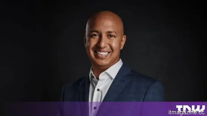 The upcoming challenge in fintech is to comprehend the individual behind the data.
Amr Mohamed, the founder of Neumetria, believes that fintech requires a behavioral understanding layer that explains the reasons behind transactions, rather than merely detailing what they are. As AI agents integrate into financial systems, the importance of context as a foundational element grows.
The upcoming challenge in fintech is to comprehend the individual behind the data.
Amr Mohamed, the founder of Neumetria, believes that fintech requires a behavioral understanding layer that explains the reasons behind transactions, rather than merely detailing what they are. As AI agents integrate into financial systems, the importance of context as a foundational element grows.
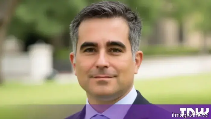 As artificial intelligence transforms the business landscape, the role of the fractional CTO is becoming increasingly relevant.
Only 21% of businesses have developed mature AI governance, while 74% anticipate utilizing agents by 2027 (Deloitte). Daniel Kirichanski, founder of Prime Path Global, contends that fractional CTO leadership addresses the divide between AI aspirations and organizational preparedness.
As artificial intelligence transforms the business landscape, the role of the fractional CTO is becoming increasingly relevant.
Only 21% of businesses have developed mature AI governance, while 74% anticipate utilizing agents by 2027 (Deloitte). Daniel Kirichanski, founder of Prime Path Global, contends that fractional CTO leadership addresses the divide between AI aspirations and organizational preparedness.
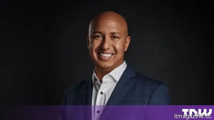 The upcoming challenge in fintech is gaining insight into the individual behind the data.
Amr Mohamed, the founder of Neumetria, contends that fintech requires a layer focused on behavioral understanding to explain the reasons behind transactions, rather than merely identifying them. As AI agents integrate into financial systems, context transforms into a fundamental component.
The upcoming challenge in fintech is gaining insight into the individual behind the data.
Amr Mohamed, the founder of Neumetria, contends that fintech requires a layer focused on behavioral understanding to explain the reasons behind transactions, rather than merely identifying them. As AI agents integrate into financial systems, context transforms into a fundamental component.
 Anthropic is evaluating a new standard for Claude to interface with factory and laboratory equipment.
Anthropic's Model Hardware Standard allows vendors to define how an AI can control a machine. Starting in January 2027, Europe will oversee the safety features of AI in machinery.
Anthropic is evaluating a new standard for Claude to interface with factory and laboratory equipment.
Anthropic's Model Hardware Standard allows vendors to define how an AI can control a machine. Starting in January 2027, Europe will oversee the safety features of AI in machinery.
 As artificial intelligence transforms the business landscape, the role of the fractional CTO is becoming increasingly relevant.
Only 21% of organizations have established mature AI governance, while 74% anticipate utilizing agents by 2027 (Deloitte). Daniel Kirichanski, founder of Prime Path Global, suggests that fractional CTO leadership bridges the divide between AI aspirations and organizational preparedness.
As artificial intelligence transforms the business landscape, the role of the fractional CTO is becoming increasingly relevant.
Only 21% of organizations have established mature AI governance, while 74% anticipate utilizing agents by 2027 (Deloitte). Daniel Kirichanski, founder of Prime Path Global, suggests that fractional CTO leadership bridges the divide between AI aspirations and organizational preparedness.
 The future of executive assistance: DonnaPro’s strategy for human-AI teamwork.
DonnaPro prepares executive assistants on AI tools before their commencement and supports them with 2,500 pages of frameworks. Founder Filip Pesek contends that even the most effective AI tools require a human who understands how to think critically.
The future of executive assistance: DonnaPro’s strategy for human-AI teamwork.
DonnaPro prepares executive assistants on AI tools before their commencement and supports them with 2,500 pages of frameworks. Founder Filip Pesek contends that even the most effective AI tools require a human who understands how to think critically.
SK Hynix has started construction on a $4 billion memory packaging facility in Indiana.
SK Hynix has begun construction on a $4 billion advanced packaging facility in Indiana. Europe granted state aid for a similar plant but then forfeited it.