
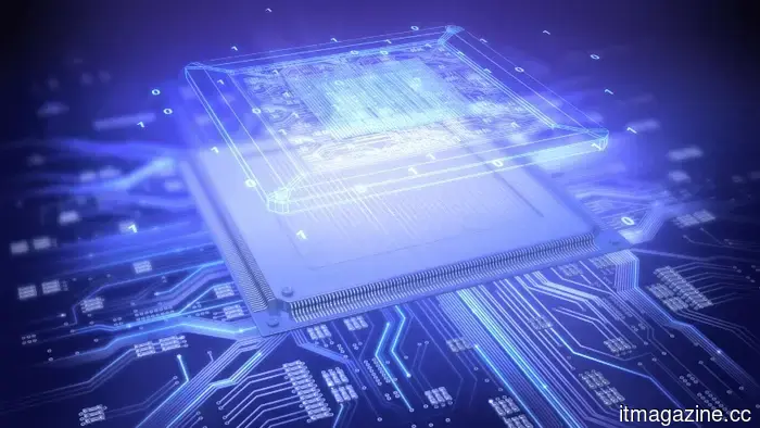
Google forms a four-partner chip supply chain with Broadcom, MediaTek, and Marvell to compete with Nvidia in inference.
Summary: Google is establishing the AI industry's most varied custom chip supply chain by collaborating with four design partners (Broadcom, MediaTek, Marvell, Intel) and has a roadmap that includes the Ironwood TPU, which is currently being shipped in the millions, leading up to the TPU v8 chips at TSMC's 2nm technology, anticipated for late 2027. This strategy, outlined prior to Google Cloud Next, distinguishes the next generation clearly: Broadcom’s “Sunfish” will be used for training, while MediaTek’s “Zebrafish” is intended for inference at a cost reduction of 20-30%. Additionally, Marvell is in discussions to introduce a memory processing unit and another inference TPU, positioning Google's custom silicon as a significant challenge to Nvidia's leadership in AI inference.
Google is creating the most diversified custom chip supply chain within the AI sector, involving four design partners, a fabrication agreement with TSMC, and a product roadmap extending from current inference chips to the anticipated 2-nanometre processors expected in late 2027. This approach, elaborated in a Bloomberg article ahead of Google Cloud Next, aims to position Google’s silicon initiative as the main competitor to Nvidia's authority in AI inference, which is the stage of computing where models cater to users instead of learning from data.
The key component is Ironwood, Google’s seventh-generation TPU, specifically designed for inference purposes. It delivers ten times the peak performance of the TPU v5p, features 192 gigabytes of HBM3E memory per chip with a bandwidth of 7.2 terabytes per second, and can scale up to 9,216 liquid-cooled chips in a single superpod, achieving 42.5 FP8 exaflops. Ironwood is now generally accessible to Google Cloud customers, with plans to produce millions of units this year, and Anthropic has agreed to acquire up to one million TPUs. Meta also has an arrangement to rent these units.
Google’s chip initiative currently encompasses four unique design partners, each responsible for various aspects of the product line. Broadcom, which secured a long-term contract on April 6 to supply TPUs and networking components through 2031, will manage the high-performance chip variants and is designing the next-generation TPU v8 training chip, codenamed “Sunfish,” aimed at TSMC’s 2-nanometre process for late 2027. Broadcom holds over 70% of the custom AI accelerator market and anticipates generating $100 billion in AI chip revenue by 2027.
MediaTek is developing the cost-optimized inference version of the TPU v8, dubbed “Zebrafish,” also targeting TSMC 2nm for late 2027. MediaTek’s engagement began with the I/O modules and peripheral components for Ironwood, which allow for designs that are 20 to 30% more cost-effective than alternatives. The TPU v8 strategy clearly delineates the product line: Broadcom focuses on the training chip while MediaTek concentrates on the inference chip, thus providing Google with negotiation leverage since each partner is aware of the other’s contributions.
Marvell Technology is negotiating with Google to create a memory processing unit and a new inference-centric TPU, which would mark them as the third design partner if successful. Google aims to manufacture nearly two million memory processing units, with designs anticipated to be finalized by the following year. Marvell's custom silicon business is operating at a $1.5 billion annual rate with 18 design wins from cloud providers, and Nvidia has invested $2 billion into the company in March.
Intel became involved on April 9 with a multi-year agreement to supply Xeon processors and custom infrastructure processing units for Google’s AI data center needs. This partnership focuses on the networking and general-purpose computing layers surrounding the TPUs rather than the AI accelerators themselves.
TSMC is responsible for fabricating all of Google’s custom silicon. The collaboration is fundamental: all chips designed by Google, regardless of the partner, are processed through TSMC’s facilities.
Understanding the economics of inference
The transition from training to inference as the primary cost in AI computing is the strategic foundation of Google's chip program. Training a leading-edge model is a unique, resource-intensive event, while inference is ongoing, scaling with every user, query, and AI-integrated product. Google handles billions of AI-enhanced search queries, Gemini conversations, and daily Cloud AI API calls. At this level, the cost per inference is critical to the overall economics of the AI industry.
Nvidia’s GPUs still dominate training workloads due to their programmability and the CUDA software ecosystem, which establishes switching costs that custom chips struggle to replicate. Conversely, inference workloads are more consistent and repetitive, making them suitable for the fixed-function optimization that custom silicon handles well. A purpose-built inference chip that offers cost advantages over an Nvidia GPU, even lacking the GPU’s versatility, is
Altri articoli
 Il film di Elden Ring ha appena ricevuto una data di uscita, un cast eccezionale, e si sta girando in IMAX.
L'adattamento di Elden Ring di A24 è ora in produzione nel Regno Unito, diretto da Alex Garland. George R.R. Martin ha co-scritto la mitologia del gioco ed è ora produttore del film live-action.
Il film di Elden Ring ha appena ricevuto una data di uscita, un cast eccezionale, e si sta girando in IMAX.
L'adattamento di Elden Ring di A24 è ora in produzione nel Regno Unito, diretto da Alex Garland. George R.R. Martin ha co-scritto la mitologia del gioco ed è ora produttore del film live-action.
 Motorola ha appena aperto la beta di Android 17 a più telefoni Razr ed Edge.
Motorola sta ampliando l'accesso alla beta di Android 17 a più telefoni premium, aggiungendo due modelli Razr e l'Edge 50 Ultra in diverse regioni.
Motorola ha appena aperto la beta di Android 17 a più telefoni Razr ed Edge.
Motorola sta ampliando l'accesso alla beta di Android 17 a più telefoni premium, aggiungendo due modelli Razr e l'Edge 50 Ultra in diverse regioni.
 8 migliori piattaforme di software per la gestione dei fornitori per il 2026
Confronta le migliori piattaforme software per la gestione dei fornitori per il 2026, comprese le capacità di intelligenza artificiale, gli strumenti di conformità e le funzionalità per unificare i dati sui fornitori, i contratti e le spese.
Google compone una catena di fornitura di chip a quattro partner con Broadcom, MediaTek, Marvell per sfidare Nvidia nell'inferenza.
Il programma di chip personalizzati di Google coinvolge quattro partner di design e una roadmap TPU v8 a doppio binario presso TSMC 2nm, posizionando il suo silicio per l'inferenza come la sfida più diretta a Nvidia.
8 migliori piattaforme di software per la gestione dei fornitori per il 2026
Confronta le migliori piattaforme software per la gestione dei fornitori per il 2026, comprese le capacità di intelligenza artificiale, gli strumenti di conformità e le funzionalità per unificare i dati sui fornitori, i contratti e le spese.
Google compone una catena di fornitura di chip a quattro partner con Broadcom, MediaTek, Marvell per sfidare Nvidia nell'inferenza.
Il programma di chip personalizzati di Google coinvolge quattro partner di design e una roadmap TPU v8 a doppio binario presso TSMC 2nm, posizionando il suo silicio per l'inferenza come la sfida più diretta a Nvidia.
 Gemini Live riceve un redesign dell'app minimalista che ti consente di fare di più
Google ha ridisegnato Gemini Live con un'interfaccia più pulita, rendendo le conversazioni AI più fluide e più facili da accedere all'interno dell'app principale.
Gemini Live riceve un redesign dell'app minimalista che ti consente di fare di più
Google ha ridisegnato Gemini Live con un'interfaccia più pulita, rendendo le conversazioni AI più fluide e più facili da accedere all'interno dell'app principale.
 Il Framework di Visibilità del Marchio di Semrush viene lanciato all'Adobe Summit mentre la ricerca AI riscrive le regole della scoperta.
Il nuovo framework di Semrush introduce l'ottimizzazione della ricerca agentica e si basa su 213 milioni di prompt LLM per misurare la visibilità del marchio nelle ricerche AI, mentre il CTR organico diminuisce del 61%.
Il Framework di Visibilità del Marchio di Semrush viene lanciato all'Adobe Summit mentre la ricerca AI riscrive le regole della scoperta.
Il nuovo framework di Semrush introduce l'ottimizzazione della ricerca agentica e si basa su 213 milioni di prompt LLM per misurare la visibilità del marchio nelle ricerche AI, mentre il CTR organico diminuisce del 61%.
Google forms a four-partner chip supply chain with Broadcom, MediaTek, and Marvell to compete with Nvidia in inference.
Google's custom chip initiative involves four design partners and a dual-track TPU v8 roadmap at TSMC's 2nm process, making its inference silicon a significant competitor to Nvidia.