
Huawei presents the 'Tau Scaling Law' as China’s solution to circumvent US chip sanctions.
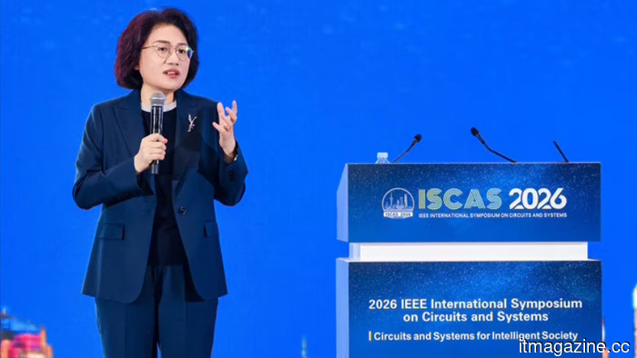
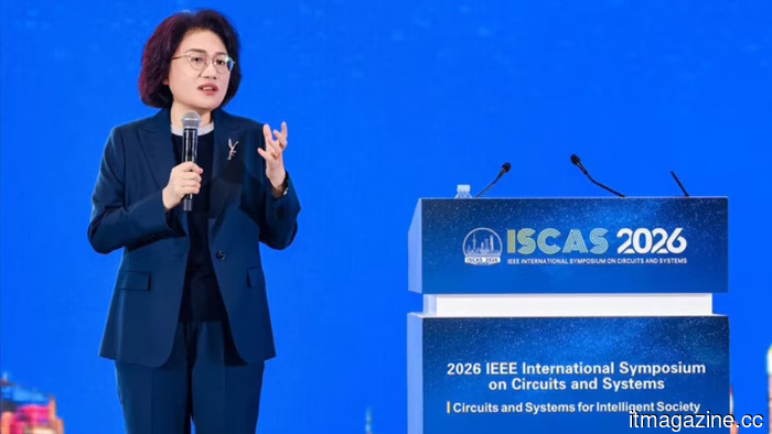
He Tingbo, during a keynote in Shanghai, asserted that the new frontier in technology lies in reducing signal-propagation time rather than in shrinking transistors, revealing that Huawei has been secretly developing chips based on this concept for the past six years. On the opening day of the IEEE International Symposium on Circuits and Systems in Shanghai, Huawei argued that the global semiconductor industry requires a new organizational principle and claims to have one ready.
He Tingbo, who leads Huawei’s semiconductor division and chairs its Scientist Committee, told attendees that the company has spent six years working on what it terms the Tau (τ) Scaling Law, which is now being implemented across its chip lineup. The central assertion is that geometric scaling—the continuous reduction of transistors that has directed the industry for over fifty years—is no longer effective.
According to the announcement, the τ Scaling Law focuses on the time it takes for signals and data to travel through a chip and its corresponding system during the design process. The premise is that by shortening this time, performance and effective transistor density can be enhanced without relying on manufacturing advances from which Huawei has been blocked.
In his keynote titled "New Semiconductor Path in Practice," He introduced an architecture named LogicFolding, which Huawei claims reorganizes circuit layouts to minimize critical-path wiring and lessen the resistive and capacitive burden on signal propagation. The Kirin chips set to launch this autumn will be the first to feature this technology, according to the company.
A long-term projection is set for 2031, when Huawei anticipates designing high-end chips with transistor densities comparable to a 1.4-nanometer process, a target most of the industry expects to achieve by the end of the decade through extreme ultraviolet lithography, technology that Chinese companies are prohibited from buying. Huawei has not released independent performance data to support this claim.
Over the past six years, He indicated that Huawei has designed and mass-produced 381 chips based on the τ principle for applications in smartphones, AI computing, and other unspecified categories. This assertion is currently exclusive to Huawei, with no external verification of the figure.
This situation unfolds against a familiar backdrop, as Washington has spent four years tightening export controls on the lithography tools, design software, and high-bandwidth memory essential for the most advanced nodes, with ASML—the Dutch manufacturer of the EUV systems that Huawei needs for conventional 1.4 nm production—barred from exporting its most advanced equipment to China. The MATCH Act being discussed in Washington could further tighten restrictions. In response, Huawei is working to design around these constraints instead of waiting for them to lift.
The company has been publicly laying the groundwork for this argument for months. A tour of its secret chip lab featured on Chinese state television in late October, two days before Donald Trump's visit to Beijing, highlighted the geopolitical implications. The keynote on Monday addressed the technical aspects. He Tingbo, sometimes noted in the Chinese media as the country’s “chip queen,” has been leading Huawei’s semiconductor initiatives since 2003 and currently represents the push for self-reliance.
Whether the τ Scaling Law constitutes a coherent design philosophy or merely a rebranding of established circuit-level optimization techniques remains to be determined. Huawei framed the announcement as an open invitation, with He encouraging scientists, engineers, and industry partners worldwide to collaborate on the initiative. Practically, the audience for this invitation primarily resides within China.
The first tangible test will occur this autumn when the Kirin chips are made available to consumers, while the longer-term vision extends to 2031.
Other articles
 Uber fully pursues Delivery Hero with an offer that is lower than the closing price.
Delivery Hero has verified Uber's takeover proposal of €33 per share, which amounts to approximately $11 billion, coinciding with DoorDash's consideration of its own offer and the CEO's plans to resign.
Uber fully pursues Delivery Hero with an offer that is lower than the closing price.
Delivery Hero has verified Uber's takeover proposal of €33 per share, which amounts to approximately $11 billion, coinciding with DoorDash's consideration of its own offer and the CEO's plans to resign.
 Uber targets Delivery Hero in its entirety, making an offer that is below the closing price.
Delivery Hero has confirmed Uber's takeover proposal of €33 per share, which places its valuation at approximately $11 billion, while DoorDash is considering its own offer and the CEO is getting ready to resign.
Uber targets Delivery Hero in its entirety, making an offer that is below the closing price.
Delivery Hero has confirmed Uber's takeover proposal of €33 per share, which places its valuation at approximately $11 billion, while DoorDash is considering its own offer and the CEO is getting ready to resign.
 The ECB gathers banks to discuss AI cybersecurity threats stemming from Mythos.
The ECB is urging banks to address vulnerabilities more swiftly as Anthropic's Mythos uncovers thousands of zero-day flaws, while European lenders continue to be excluded from testing.
The ECB gathers banks to discuss AI cybersecurity threats stemming from Mythos.
The ECB is urging banks to address vulnerabilities more swiftly as Anthropic's Mythos uncovers thousands of zero-day flaws, while European lenders continue to be excluded from testing.
 SoftBank reaches a new high as Tokyo anticipates the upcoming OpenAI IPO.
On Monday, SoftBank's shares reached an all-time high, propelling the Nikkei above 65,000 for the first time, coinciding with reports that OpenAI's IPO filing is approaching.
SoftBank reaches a new high as Tokyo anticipates the upcoming OpenAI IPO.
On Monday, SoftBank's shares reached an all-time high, propelling the Nikkei above 65,000 for the first time, coinciding with reports that OpenAI's IPO filing is approaching.
 ECB gathers banks to discuss AI cybersecurity threats posed by Mythos.
The ECB is urging banks to address vulnerabilities more quickly as Anthropic's Mythos discovers thousands of zero-day flaws, while European lenders continue to be excluded from testing.
ECB gathers banks to discuss AI cybersecurity threats posed by Mythos.
The ECB is urging banks to address vulnerabilities more quickly as Anthropic's Mythos discovers thousands of zero-day flaws, while European lenders continue to be excluded from testing.
Huawei presents the 'Tau Scaling Law' as China’s solution to circumvent US chip sanctions.
During an ISCAS keynote in Shanghai, Huawei's He Tingbo presented the Tau Scaling Law, a chip-design methodology centered on signal timing rather than the size of transistors.